Today, silicon carbide is used in demanding semiconductor applications such as trains, turbines, electric vehicles, and smart grids. Due to their physical and electrical properties, sic based devices are suitable for applications with high temperature, high power density and high operating frequencies. While SiC power devices are capable of advancing in demanding areas such as electric vehicles, 5G, and iot technologies, the production of high-quality SiC substrates presents multiple challenges for wafer manufacturers.
Surprisingly, the greatest potential is still ahead of us. Silicon-based semiconductors, the foundation of the technology, will continue to make significant advances in various fields including automotive, consumer electronics, aerospace, and medicine. Currently, automotive applications dominate the SiC market, accounting for more than 75% of the total power SiC device market. The accelerated adoption of SiC leads to a compound annual growth rate of 34% during the forecast period 2021-2027.
Silicon carbide applications
SiC is the substrate material of choice for advanced semiconductors, especially power electronics, to meet the growing demands of electronic devices. It allows 15 times higher breakdown voltage, 10 times stronger dielectric breakdown field and 3 times stronger thermal conductivity. In addition, SiC has a high current density of 2 to 3 times and allows for higher operating temperatures (up to 400°C compared to 150°C for silicon).
SiC semiconductors are in higher demand in a variety of industries due to their performance at high temperatures, voltages and power levels. For example, SiC power supplies are used in data centers to significantly reduce the amount of power required for cooling systems. The uninterruptible power supply system also guarantees a continuous and reliable source of power. Another application is the increased power demand of 5G base stations, which need to process more and more data. SiC semiconductors provide higher power in a smaller size and are used in megahertz switches.
Good for the auto industry
The automotive industry benefits from the advantages of SiC in the following applications:
● In-car battery chargers: In this application, SiC can double the power and half the size.
● On-board DC/DC Converter :SiC is used to convert on-board battery voltage into a clean 12vdc bus to power on-board devices.
● Powertrain: Here, SiC helps to reduce switching losses to less than 80% and size reduction by 30%. This makes the battery smaller (lighter weight, less heat) and lasts longer.
● Car DC fast charging station
The biggest hurdle for the industry comes not only from the number of wafers needed to meet demand over the next five years, but also from modifying wafer parameters to match those of silicon wafers. Current and next-generation production technologies will be driven by tighter tolerances and standards. To overcome these obstacles, innovation is essential.
SiC manufacturing solutions from Pureon
Since the market is aiming for power device prices to match those of silicon-based devices, SiC substrate producers have an incentive to improve process efficiency and reduce wafer production costs. In addition, SIC-based applications and all other types of semiconductors are in very high demand, requiring innovation in the manufacturing process.
Most manufacturers believe that reducing processing time or using cheaper consumables will save costs. However, a significant reduction in the cost of ownership will be achieved through increased production. The entire manufacturing process is influenced by consumables and surface treatment options. In the process of optimizing yield, uniformity of pad, paste and template between each batch is critical. Two decades of product development for the SiC market and Pureon's semiconductor experience have helped the company overcome manufacturing barriers.

Figure 1: Manufacturing SiC wafers (Source: Pureon)
Solutions to optimize and increase production
Pureon conducts testing and generates data through its own polishing and surface laboratory, as it is a consumable manufacturer with in-house wafer processing capabilities. This feature provides customers with representative data to reduce the risk of new product testing and certification, and significantly reduces Pureon's development cycle. As a result, the testing and acceptance process at wafer manufacturer factories is accelerated.
Wafers with a diameter of 200 mm require entirely new manufacturing processes and machinery. New manufacturing techniques are introduced at each stage of the process to create high-volume manufacturing processes that meet these new requirements. Pureon is ideally positioned to provide SiC wafer manufacturers with next-generation solutions to mature the market by increasing productivity and reducing cost of ownership. Pureon's solutions reduce cycle times, extend consumable life, optimize and increase production.
Where is Pureon's solution used
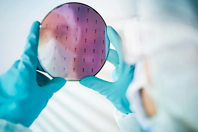
Wafer billets of single crystals or ingots must first be cut to prepare the SiC substrate for device manufacturing. The main way to achieve this is to use a multi-wire saw and high-speed running thin wire with diamond abrasive paste to precisely cut the wafer billet on the SiC ingot. Figure 1 shows the general process flow of SiC wafer fabrication.
In the process of manufacturing wafers, the in-line saw step to successfully cut a high-quality blank is probably the most critical step, as the later wafer shape enhancement is very challenging. When it comes to the wire sawing process, Pureon offers oil-based and non-oil-based corundum abrasive pulp as an option. To further improve this process, Pureon works closely with wire saw Oems and customers. The mud's proprietary chemical composition and classified diamonds ensure lot-to-lot uniformity, resulting in repeatable processes at customer sites and improved wafer yield and quality.
High surface quality and impressive inventory removal rates
Mechanical polishing of wafers using a polishing paste containing diamonds and polishing pads is the next important step in the production of SiC substrates. A typical process is performed on a combination of double-sided, single-sided or double-sided and single-sided polishing tools. The result of this production step is that the wafer is very flat and has a low level of roughness when it is ready for final polishing.
Manufacturing diamond-based grout has long been a priority for the innovation team at Bonhams. The company has discovered highly optimized formulations that can regulate material removal rates on various SiC substrate surfaces. Pureon has developed a new solution for grinding SiC wafers that achieves both high surface quality and impressive removal rates.

Better results with CMP polishing pads
Chemical mechanical polishing (CMP) is the name for the last significant stage in the manufacture of SiC wafers. This process step has the sole purpose of preparing the substrate surface for epitaxial growth, with no or little wafer-shape modification. This is normally accomplished by removing only a few microns from the wafer surface using a highly reactive chemical polishing slurry and a polyurethane-based or urethane-impregnated felt-type polishing pad. In single-side batch tools, wafers are transported to the polishing pad and secured using a template. In single-wafer tools, wafers are secured using a vacuum chuck and a backing film. These wafer carriers’ materials must have strong resistance to the highly reactive chemistry of the polishing slurry, as they are exposed to it.
To improve cost of ownership and increase service life, Pureon keeps creating cutting-edge wafer templates and films for use in this process. Two new polishing pads for SiC CMP have been released to the market thanks to tight collaboration between Pureon and the industry. The CMP procedure is now more productive and produces better results thanks to these new CMP polishing pads.
Conclusion
Significant improvements in substrate production, both in its current form and in the creation of next-generation substrates, are necessary to support the expansion of the SiC device market. For nearly 20 years, Pureon has provided the SiC wafering sector with support through its knowledge, products and expertise in this space. Pureon’s specialists keep coming up with new ideas, increasing substrate yields and bringing down the price of SiC wafers, allowing this technology to be used more quickly.
About US