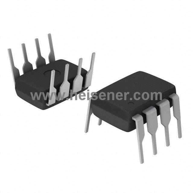
The TC6320 consists of an 8-pin SOIC and a high-voltage, low-threshold N-channel and P-channel MOSFETs in DFN packaging. Both MosFeTs incorporate gate-to-source resistors and gate-to-source Zener diode clips, which are required for high-voltage pulse generator applications. It is a free, high speed, high voltage, grid-clamped n-channel and P-channel MOSFET pair using an advanced vertical DMOS structure and a proven silicon gate manufacturing process.
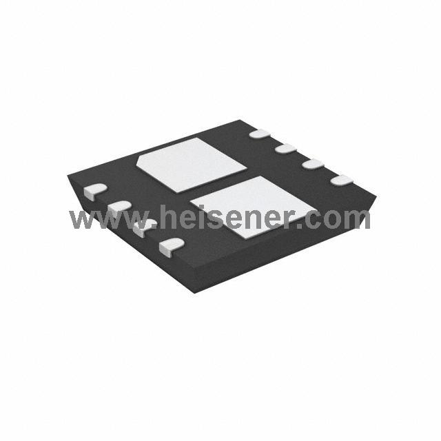
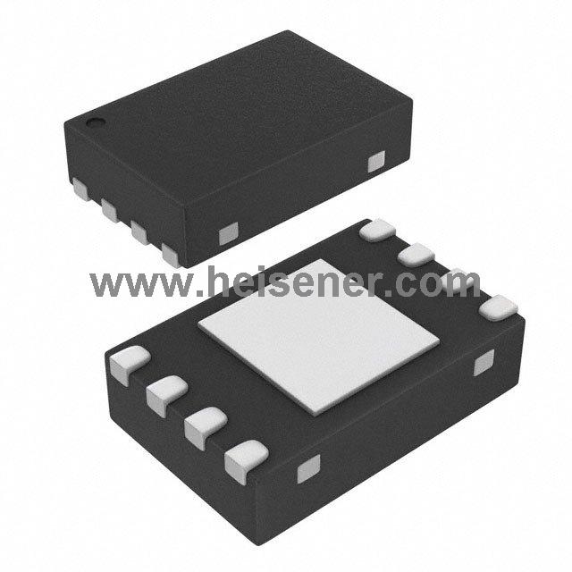
Type of package

This combination results in devices with the power processing capabilities of bipolar transistors and with the high input impedance and positive temperature coefficient inherent in MOS devices. The device has all the characteristics of the MOS structure without thermal runaway and heat-induced secondary breakdown.
Functional Block Diagram

Microchip's vertical DMOS FeTs are ideal for a wide range of switching and amplification applications that require very low threshold voltages, high breakdown voltages, high input impedance, low input capacitance, and fast switching speeds.
Typical Application Circuit

Features
• Integrated Gate-to-source Resistor
• Integrated Gate-to-source Zener Diode
• Low Threshold
• Low On-resistance
• Low Input Capacitance
• Fast Switching Speeds
• Free from Secondary Breakdown
• Low Input and Output Leakage
• Independent Electrically Isolated N-channel and P-channel
Applications
• High-voltage Pulsers
• Amplifiers
• Buffers
• Piezoelectric Transducer Drivers
• General Purpose Line Drivers
• Logic-level Interfaces