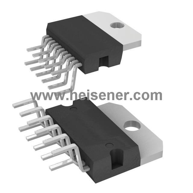
TDA2009A Description
The TDA2009A is a class AB dual Hi-Fi audio power amplifier designed for delivering high-quality sound performance in stereo applications. Housed in a compact Multiwatt® package, this amplifier is ideal for use in Hi-Fi systems, music centers, and similar audio devices.
Key features of the TDA2009A include dual-channel operation for stereo sound, robust thermal stability, and built-in protection against short circuits and thermal overloads. These features enhance its reliability and make it a popular choice for audio enthusiasts and manufacturers seeking consistent performance in stereo audio amplifiers.
TDA2009A Symbol

TDA2009A Footprint
[
TDA2009A 3D Model

TDA2009A Pin Connection

NON INY. INPUT (1): Non-inverting input for channel 1, used to receive the audio signal for amplification.
INY. INPUT (1): Inverting input for channel 1, typically connected for feedback or differential signal input.
SVRR (Supply Voltage Rejection Ratio): Pin used for power supply noise rejection, ensuring stable audio performance.
INY. INPUT (2): Inverting input for channel 2, similar to pin 2 but for the second channel.
NON INY. INPUT (2): Non-inverting input for channel 2, for the second audio channel.
GND (Ground): Common ground connection for the amplifier, ensuring proper electrical reference.
N.C. (No Connection): Pin not internally connected, reserved or unused.
OUTPUT (2): Amplified output for channel 2, providing enhanced audio signal.
VS+ (Positive Supply Voltage): Positive voltage supply pin for powering the amplifier.
OUTPUT (1): Amplified output for channel 1, providing enhanced audio signal.
N.C. (No Connection): Another pin without an internal connection, unused in the design.
TDA2009A Schematic Diagram

TDA2009A Test and Application Circuit

TDA2009A Specification
| Parameter | Specification |
| Supply Voltage (Vs) | 8V ~ 28V |
| Output Power | Up to 10W per channel at 8Ω load, 1% THD |
| Max Output Power x Channels @ Load | 12.5W x 2 @ 4Ohm |
| Operating Temperature | -40°C ~ 150°C |
| Quiescent Current | 50 mA |
| Input Impedance | High (typical ~100kΩ) |
| Frequency Response | 20 Hz to 20 kHz (Hi-Fi audio range) |
| Total Harmonic Distortion | 0.1% (typical at 1W, 1 kHz) |
| Voltage Gain | 30 dB |
| Channel Separation | 50 dB |
| Output Load Impedance | 4Ω or 8Ω |
| Slew Rate | 1.5 V/µs |
| Package | Multiwatt-11 |
TDA2009A Features
HIGH OUTPUT POWER (10 + 10W Min. @ D = 1%)
HIGH CURRENT CAPABILITY (UP TO 3.5A)
AC SHORT CIRCUIT PROTECTION
THERMAL OVERLOAD PROTECTION
SPACE AND COST SAVING : VERY LOW NUMBER OF EXTERNAL COMPONENTS AND SIMPLE MOUNTING THANKS TO THE MULTIWATT PACKAGE.
TDA2009A Applications
Stereo Audio Systems
Television Audio Output
Multimedia Speaker Systems
Car Audio Systems
Portable Audio Equipment
Public Address Systems
DIY Audio Projects
TDA2009A Package
The TDA2009A is housed in a Multiwatt-11 package, a robust design optimized for high-power audio applications. This package features 11 pins arranged in a single row, ensuring straightforward integration into through-hole PCBs. Constructed from thermally conductive materials, the package supports efficient heat dissipation, making it ideal for amplifiers operating under high power.
In terms of dimensions, the Multiwatt-11 package measures approximately 20 mm in length, 16 mm in width, and 8.5 mm in height, with a standard pin pitch of 2.54 mm. The integrated heat sink tab enhances thermal management, allowing for reliable operation in demanding environments.
How to Use TDA2009A?
Using the TDA2009A is straightforward, but attention to a few key steps is essential. First, ensure the chip's supply voltage is within the recommended range and add filter capacitors at the power input to minimize noise interference. Next, connect the input signals to the non-inverting input pins based on the circuit design, while the inverting input pins should be connected to the feedback circuit, usually configured with a combination of resistors and capacitors. Additionally, the ground pin must be securely connected to the audio system's ground to avoid noise issues.
When connecting the output pins (pins 8 and 10) to the speakers, it is advisable to add a protective circuit, such as a series combination of an appropriate resistor and capacitor, to prevent transient currents from damaging the speakers or the chip itself. Furthermore, the heatsink at the bottom of the chip must make firm contact with a heat dissipation surface, enhanced with thermal grease to improve efficiency. Before powering up, thoroughly check all connections to ensure correctness and avoid short circuits or wiring errors.
FAQs
What is the TDA2009A used for?
The TDA2009A is a Class AB dual Hi-Fi audio power amplifier designed for high-quality stereo applications such as Hi-Fi systems, music centers, and home audio equipment.
Does the TDA2009A require additional components for operation?
Yes, the TDA2009A requires external components such as decoupling capacitors, feedback resistors, and protective circuitry for the outputs.
What precautions should be taken during installation?
Ensure proper grounding of pin 6, add filter capacitors to the power supply, and attach a heat sink with thermal grease to the chip's backplate for effective heat dissipation. Also, check all connections thoroughly before powering up to avoid damage.